Modify Your Composite LCD to Work at 5v
This guide was updated on 2/7/17
To purchase a 4.3″ LCD with the following process already completed, visit the store.
If your LCD controller is not exactly like the one shown here, visit the forum and look for one that matches.
Background
Composite LCDs are great for Raspberry Pi projects. They are cheap and very easy to attach. The only problem is that most of them are made to work at 12v. Some of them work decently at 5v, but most only work properly between 6-12v and the ones that do work at 5v usually work very inefficiently.
This tutorial will show a method of adapting the driver to work at 5v, matching the operating voltage of the Raspberry Pi. This tutorial applies specifically to boards with this version of the 1509 5.0v buck converter only. LCD’s with other buck converters may function a similar manner, but the pinouts or voltages may be different. Please do research before proceeding if you have a different component. Visit the forum to find your’s.
The Process
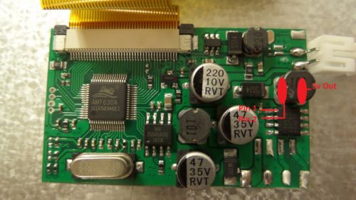
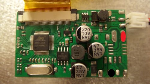
Here is a typical driver board for a composite LCD. This the driver for the 4.3″ LCD that’s used in the PSPi projects. It has 4 inputs: +12v In, GND, composite 1, and composite 2.
The process of adapting any of these boards starts by doing some research. We have to figure out what components are taking 12v and converting it to the voltages that the LCD uses. I’ll save you some trouble now and tell you that there are multiple voltage convertions on these boards, and we are only looking for the initial major convertion. Some of these boards drop the voltage to 5v initially (like the one shown), and then drop to 3.3v in other areas to power the main components. Some of the drop to 3.3v from the beginning and skip 5v altogether.[spacer height=”1px”]
We have to figure out which component is doing the initial voltage drop. Let’s trace out the +12v power path and see where it is headed. The left pad is the +12v input and it’s only routed through one path, starting with a large diode. After the diode we have an inductor (labeled 101), and from there the PCB trace leads to the top left pin of this 8-pin component. This looks promising. The lettering at the top of the component is XL1509. A quick google search will bring up a datasheet for this component, which you can view here.
The datasheet tells us a few things:
- This is definitely a buck converter
- There are different versions that output at different voltages. Some are fixed at 3.3V, 5V, or 12V, and others are adjustable.
- How it’s wired to drop the voltage
So now we know that this is the buck converter, and we know that it can output many different voltages. There is some additional information written on this chip that helps us determine what voltage it drops to. Under the XL1509 there is 5.0E, telling us that it has a fixed 5v output. We aren’t going to trust this though, we must be sure.[spacer height=”1px”]
Now lets get a look at the pins. Pin 1 is labeled VIN, and the description says that it accepts input voltages of 4.5-40v. If we compare this to the PCB image above, then it looks promising. If we look at the other pins, we can see that pins 5, 6, 7, and 8 all connect together and connect to GND. That seems to match the PCB too.
[spacer height=”1px”]
Looking further into the datasheet, there is a nice diagram showing the path of power coming in through Pin 1, going out through Pin 2, and then going through a component called L1. I won’t get into what’s happening here because it’s voodoo and it will blow your mind. Just know that after this L1 component we have 5v.
[spacer height=”1px”]
Now we have to verify our information. Attach 12v to the power input and supply power to it. Use a voltmeter to verify the voltage on the output of the buck. If you compare the PCB to the schematic, you’ll see that the left ride of the inductor labeled 101 (this is L1 on the schematic) attaches to pin 2 of the buck, so that means the right side of the inductor is the output of 5v. Connect a voltmeter between GND and the right pad of the inductor, and you should see about 5v on the voltmeter[spacer height=”1px”]
 So now we know for sure that this is our buck converter, so lets remove it. I normally use a rework unit to remove components, but you can also just cut the legs and use a soldering iron to clean it up. We can also remove the inductor since it isn’t needed anymore and the pad is the perfect place to attach our new power input. I also remove the diode to the left of the inductor, since it isn’t needed anymore and can be useful for other projects.[spacer height=”1px”]
Here’s the board with all three components removed.
[spacer height=”1px”]
Once the components are removed, bypass the old circuit by attaching 5v directly to the pad we measured voltage at earlier. The GND gets connected to the same point as before.
[spacer height=”1px”]


Good tutorial
Hi,
In your “install lcd composite tutorial” you don’t mention any “hardware modification” to the driver board. And when i look at your pspi v2 pictures, the driver board hasn’t been modified.
I’m new at this and i was wondering if the component have to be desoldered in order to work with pi zero for instance.
Thanks for your answer
The LCDs I purchased in the past had a different voltage regulator and worked fine at 5v, but the new ones had a design change and no longer do. I’ve tried a dozen different vendors and everyone is selling the one shown in the picture (or one very similar).
You might get lucky and find one that works out of the box, but it’s unlikely. The one I link to in the LCD Product Page has much lower power usage than any other one I’ve used, so that’s why I chose it.
Thank you for your quick answer!
Do you think it’s possible to remove the buck converter without a rework station?
This component is really tiny and close to other smaller components.
Yes, as long as you’re careful. Holding a soldering iron on each pin and then bending them up would work. You could also cut the pins with some small side cutters and remove the chip.
Just tried it with a hobby knife^^
I cut just 4 pins on one side and then gently bent the buck converter with tweezer.
The result seems pretty nice to me, hpe it’s still working…
Keep up the good work, your projects and tutorials are really great !
I purchased a very similar board of amazon, except instead of the AP1509 my board had a XL1509-5.0E1. The two chips have the same pin configuration so I went ahead with the modification, removing the chip and adding a wire connecting the positive pad to the output. Except this doesn’t seem to have worked as my screen will not light up at all. Any thoughts?
Will you post a picture of this board and the chip in the forum? You have me curious.